
Above is an image of the receiver which was much more complicated to design than I originally thought. The methodology is as follows
- Receive data through a data line, receive clock through another data line.
- Use received clock to trigger switches to sample data from data line
- Downsample data to remove interlaced zero values
- Rebuild [4:1] vector
- Input vector into Integer to Bit
- Normalize and output through Analog Output block
Since the image above is a bit convoluted the following images will discuss eat component of the system.
Firstly, separating data.
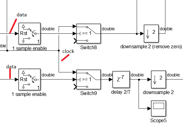
As shown above there are 2 input lines, data split between two 1 sample reset switches and the clock between two regular switches. Again the 1 sample reset switches are reset/triggered on opposite edges to help separate each channel.
The following switch is used to help select between the data line and ground. This is done so that the data comprised of A0B0A1B1A2B2 can be converted into two seperate data lines of..
- A0 0 A1 0 A2 0
- 0 B0 0 B1 0 B2
Following this a delay is applied to the second channel in order to “sync” the two channels again. I say sync, however in reality given a high enough sample rate delaying by 7 samples is essentially negligible. This is only done so that the downsample by 2 works.
Downsampling will remove the extra zeros thus creating vectors of the form A0A1A2A3…. and so on.
Secondly is the part of the system which converts the data from [1:1] to [4:1].

This is where the bulk of the processing was used and the reason why this model was so inefficient. The 8 rate transitions (4 per bit * 2 channels) and the 8 sample and holds really killed the processor. The methodology is as follows.
- Given 1 cycle of data, over 4 samples the inputs are A0A1A2A3
- Using counters that start counting from 0 to 3 and each triggering on a different value respectively we obtain 4 data lines of the following form
A0 0 0 0
0 A1 0 0
0 0 A2 0
0 0 0 A3 - In order to choose between reading a zero and a value from the data line, we use the switch which only triggers when “Hit” is observed from the counter
- The sample and holds then hold each respective value such that we can allow all 4 data lines to be sampled simultaneously to obtain a vector of [A0; A1; A2; A3] the 4 data lines will appear as follows from the output of the mux
A0 A0 A0 A0
0 A1 A1 A1
0 0 A2 A2
0 0 0 A3 - Following that using the same setup a counter and a switch is used to read the vector passing it through a ZOH and finally the bit to integer converter which converts this value back into an unsigned 4 bit integer
Lastly we have the analog output.

Luckily we do not have to do the block diagram for the DAC. The only thing done her is to scale the input, 0-15, to values of , 0-4050. Although this doesn’t increase the resolution of the output by any means, it allows one to fully use the output range of the Due’s DAC which reads uint16 numbers. Although it reads uint16 numbers only 10 of the 16 bits are used meaning that the max value is 4095.
Thus concludes the first “working” model of a dual channel transmitter and receiver which needs a clock line and digital data line.
When it came to the actual real world implementation of this, there were problems..to say the least. It was physically impossible to get the clock/data lines to be read properly due to the desynced internal clocks of two separate boards. Data was only able to be read and decomposed correctly upon multiple hard resets on the receiver board and only remained in sync for several minutes as a time.
Thus from here on out, I began to study clock recovery and various signal transmission methods to resolve this issue. In addition to that I hoped to improve the sampling rate by using a method that altered instead of each bit maybe 4 or 5 bits at a time.
Below are the receiver and transmitter simulink files. Keep in mind that I used the R2015B version of MATLAB and the same version is required to open and further edit these files i apologize for this inconvenience.
File for 1 Arduino board
To split this into two boards and try for yourself split the above file at the the 1 sample switch and use 2 digital outputs and inputs for the data stream and the clock.
